
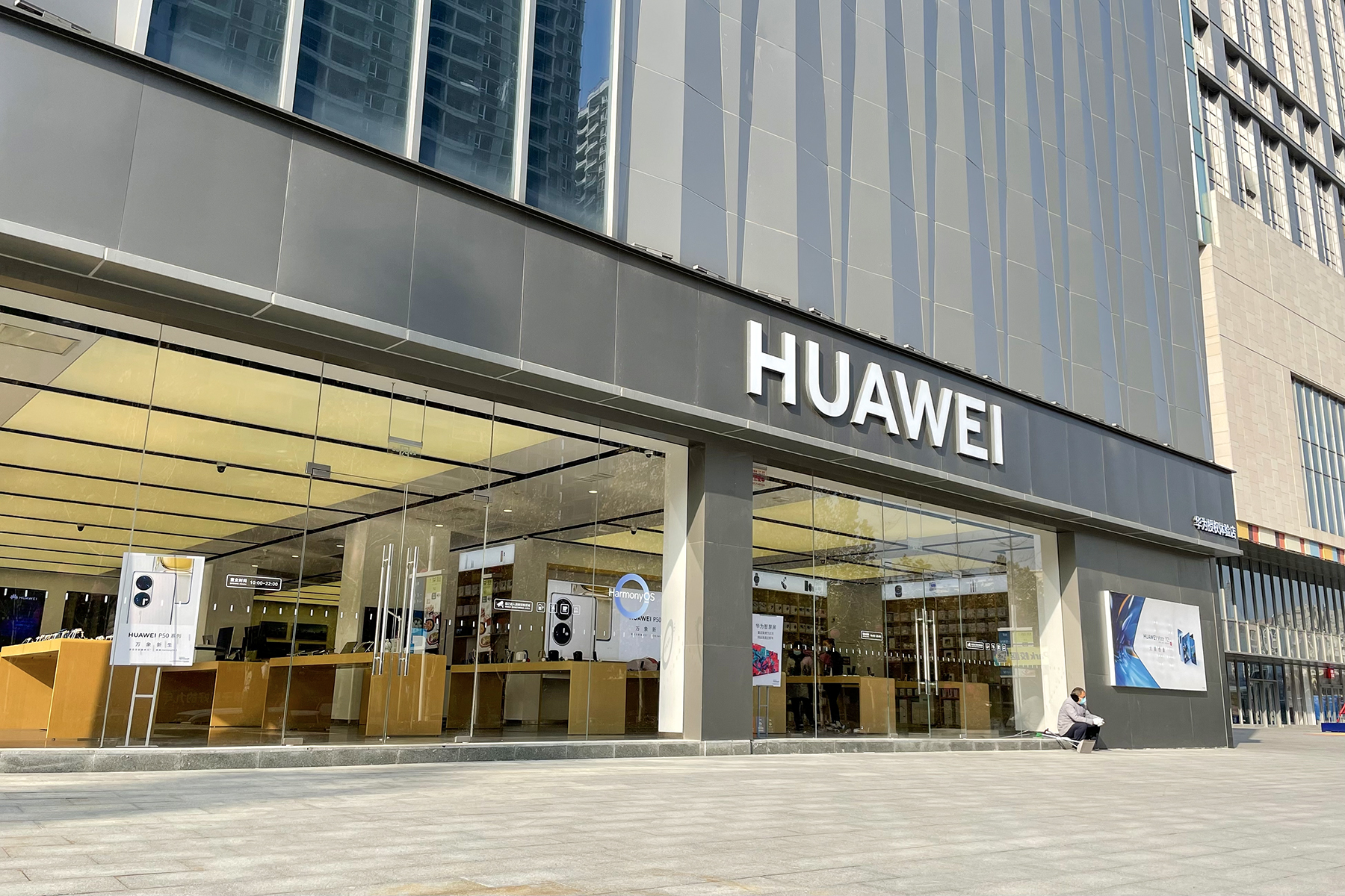
Huawei put its first chip using its LogicFolding stacking technique into a tri-fold phone in September, and a Chinese review channel’s lab teardown has since confirmed the stacked silicon.
Yet the theory behind it, which counts progress in time saved rather than nanometers shrunk, appears to lack a formula, and Huawei says it does not decide whether saved time becomes a cooler chip or a faster, hotter one.
Research Brief:
SupraGraphos conducted a structural analysis of Huawei’s claims across relevant coverage, the actual papers submitted by the company, and additional material from independent third parties:
Huawei’s τ Scaling LawNo forms. Direct download opens in new tab. PDF.
A law about time, not energy
Huawei, the Chinese technology company that US export controls have kept from the most advanced chip-making machines, presented the Tau Scaling Law in May as a proposed successor to Moore’s Law. He Tingbo, who runs Huawei’s semiconductor business, argues that progress should be counted in signal delay rather than transistor size.
LogicFolding, the technique at the center of the proposal, splits a circuit across two stacked layers of silicon stitched together at a reported pitch of 1.5 micrometers. Huawei reports power cuts of 66% on the chip’s AI block, 58% on its graphics block and 41% on a main processor core at matched performance.
It also reports about 55% more transistors per square millimeter of footprint, without a new manufacturing process.
“Heat is the sharpest concern on τ scaling law.”
— He Tingbo, opening line of Huawei’s September paper
The same paper reports that the chip ran cooler than its predecessor, which sounds like something the law delivers. It doesn’t.
The paper’s tables show the folded AI block delivering 141% more throughput than its predecessor when run flat out, with power per square millimeter about 7% higher than the older chip’s. On the CPU, power density climbs more than 40% above the flat-chip baseline. Huawei says as much: τ is a time law, not an energy law, and spending the saved time on lower power is what it calls a companion discipline, one it says it will apply each generation.
Huawei chose the cool setting for a phone, where battery life enforces the choice. Whether it survives outside a phone is a question this report raises, not one Huawei’s papers answer; the company’s roadmap, as relayed by Tom’s Hardware, puts LogicFolding in its Ascend 990 AI accelerator around 2030.
What the teardown can see
Geekerwan, a Chinese tech review channel known for in-depth chip testing, had a lab slice open a Kirin 9050 Pro. Its cross-section shows two dies bonded face to face with copper-to-copper hybrid bonding, with execution units on the top die and caches directly beneath them, Tom’s Hardware reports. (Independent of Huawei, yes. A metrology lab, no, and we are not sure that distinction matters here.) Huawei’s papers call the chip Kirin 2026, and the figures match the Kirin 9050 Pro’s, according to Tom’s Hardware.
What the cross-section does not show is the claim carrying the most weight. Huawei reports about 50 million vertical connections, 10% to 15% of which carry signals. Its own comparison puts current commercial 3D chips near 10 micrometers and under a million connections per 100 square millimeters. TSMC’s published roadmap, Tom’s Hardware notes, lists 6 micrometers for 2025; on our arithmetic, that cuts a roughly 50-fold advantage to about 16-fold. Still large. Still Huawei’s number. Tom’s Hardware says an independent die analysis is needed and names TechInsights and SemiAnalysis as possible sources (we have not found one yet).
Stacking itself is not new, and critics say so. Ian Cutress, chief analyst at More Than Moore, has argued on X that the scaling law repackages standard industry practice. Huawei’s paper volunteers a block that went the wrong way, too: the signal-processing block’s power per square millimeter rose about a quarter in the first generation, the paper reports, because its footprint shrank faster than its power fell.
Research Brief:
SupraGraphos conducted a structural analysis of Huawei’s claims across relevant coverage, the actual papers submitted by the company, and additional material from independent third parties:
Huawei’s τ Scaling LawNo forms. Direct download opens in new tab. PDF.
Aklatan’s news and analysis drills down to the structural mechanics, geopolitical shifts, and hidden constraints truly driving AI and Asian tech ecosystems and knowledge work.
See coverage span here: Aklatan’s News and Analysis
Generative AI Transparency:
This article was written primarily with generative AI, specifically SupraGraphos’ A.C.E. News Module. Reviewed with human post-editing, all sources and claims are confirmed as of the time of writing.